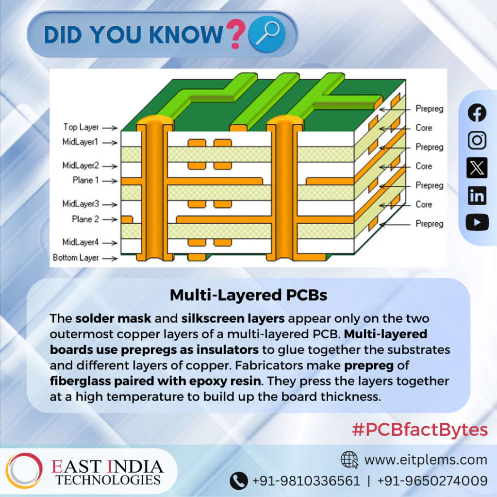
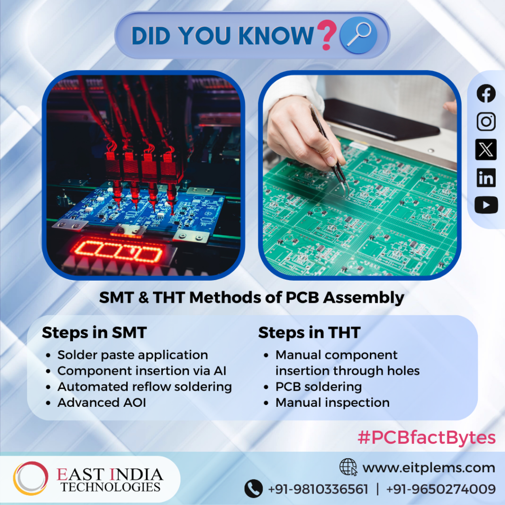
The foundation of electronic devices i.e. Printed Circuit Boards (PCBs) allow different electronic components to be connected to one another in an efficient & compact manner. In recent years, the demand for more complex and high-performance electronic devices has led to the development of advanced PCB designs. One such innovation is multi-layer PCB. Multi-layer PCB offer the advantage of way more miniaturization than ever before.
Speaking of multi-layer PCBs, we at East India Technologies provide PCB assembly services of upto 16 layered PCBs.

A 16-layered PCB is a multilayer circuit board with 16 individual layers of conductive traces, insulating layers, and ground planes. This sophisticated design offers several key benefits, some of which are listed below:
- High Density and Compactness: The multiple layers of a 16-layered PCB allow for a high density of components and interconnections. This compactness is crucial in applications like smartphones, laptops, and other miniaturized devices, where space is very limited.
- Enhanced Signal Integrity: With more layers, signal traces can be routed efficiently, reducing interference and crosstalk between components. This results in improved signal integrity and reduces electromagnetic interference, ensuring the reliable performance of the electronic device.
- Improved Thermal Management: The additional layers of a 16-layered PCB provide more room for heat dissipation. This is especially important for power-hungry devices, as it helps prevent overheating and extends the lifespan of components.
- Enhanced Power Distribution: The multiple power and ground planes in a 16-layered PCB enable efficient power distribution, reducing voltage drops and ensuring stable power supply to various components.
- High-Speed Data Transmission: The design of 16-layered PCBs is ideal for high-speed data transmission. This is crucial in applications like data servers and networking equipment, where data transfer rates are a primary concern.
- Complex Design Capabilities: The multiple layers allow for intricate and complex PCB designs, accommodating a wide range of functions and components in a single compact board.
While 16-layered PCBs offer a multitude of advantages, they also require advanced design and manufacturing expertise. Engineers need to consider factors like impedance control, layer stack-up, and thermal management to harness the full potential of this technology.
Conclusion:
Multi-layered Printed Circuit Boards (be it 10-layered PCBs or 16-layered PCBs), are a testament to the ongoing evolution of electronics. They play a pivotal role in meeting the demands of modern electronic devices, providing a miniaturized, high-performance, and reliable solution for various applications. As technology continues to advance, we can expect even more complex and capable PCB designs to emerge.
If you are looking for PCB assembly of multi-layered PCBs (upto 16 layers), then feel free to write to us at info@eitpl.com. East India Technologies Pvt Ltd is one of the leading EMS & PCB assembly service providers in India.


